LNF:Technology: Difference between revisions
Garciacortes (talk | contribs) |
Garciacortes (talk | contribs) |
||
| Line 87: | Line 87: | ||
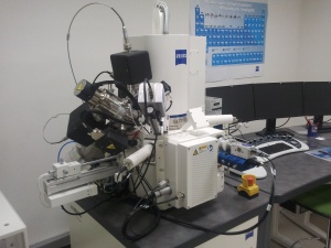
[[File:Foto0049.jpg|300px|thumb|right|FIB-SEM]] | [[File:Foto0049.jpg|300px|thumb|right|FIB-SEM]] | ||
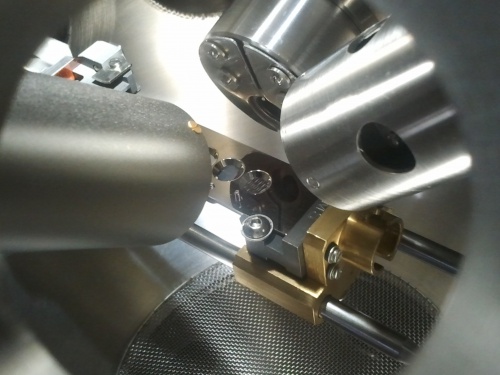
This is Carl Zeiss Auriga Compact field effect SEM with an electron acceleration voltage in the range 0.5 to 30 kV and is equipped with three different detectors for secondary and backscattered electrons. The system includes an XFlash Bruker EDS detector for compositional studies. It is possible to perform local point, line scan and mapping analysis. An electron back-scattered diffraction detector (EBSD) has been recently installed for the determination of crystalline phases and orientation with a sample angle of 70º. The microscope is also equipped with an FIB gallium gun providing an acceleration voltage of 1 to 30 keV for cross-section inspection and TEM samples preparation on conductive and insulating materials. | |||
===Secondary Ion Mass Spectrometry (SIMS)=== | ===Secondary Ion Mass Spectrometry (SIMS)=== | ||
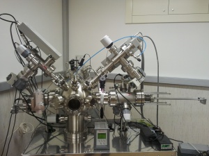
[[File:Foto0288.jpg|300px|thumb|right|SIMS]] | [[File:Foto0288.jpg|300px|thumb|right|SIMS]] | ||
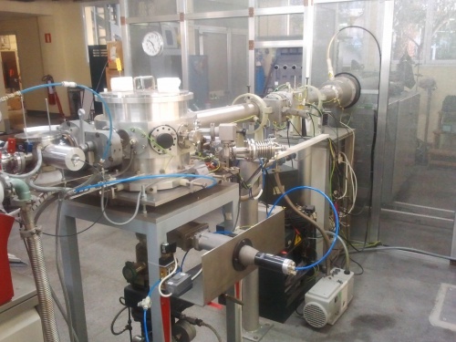
SIMS: Hiden Analytical secondary ion mass spectroscopy equipment using oxygen or argon ions as primary ions with an energy of 5 keV. Mass identification (1 to 550 amu), depth profiling and static SIMS capabilities. The system is also useful for compositional mapping and it incorporates an electron gun for SIMS experiments in insulating materials. The electronegative ions can be better detected using a Cs ion gun, with an energy up to 5 keV. | SIMS: Hiden Analytical secondary ion mass spectroscopy equipment using oxygen or argon ions as primary ions with an energy of 5 keV. Mass identification (1 to 550 amu), depth profiling and static SIMS capabilities. The system is also useful for compositional mapping and it incorporates an electron gun for SIMS experiments in insulating materials. The electronegative ions can be better detected using a Cs ion gun, with an energy up to 5 keV. | ||
Revision as of 12:29, 30 October 2015
The main mission of the Fusion Technology Division of the Spanish National Fusion Laboratory is to undertake research on the properties as well as the radiation hardness and subsequent degradation of structural and functional materials for future fusion reactors. In particular, studies on reduced activity ferritic/martensitic steels and materials used for electrical isolation, diagnostic windows etc. are central to this work. In parallel, given that at present, there is no neutron source available that simulates the fluxes and energies required for material irradiation under predicted fusion reactor conditions, the division is involved in the development of suitable neutron sources for material irradiation (ENS, IFMIF, and DONES). These sources, when on-line, will facilitate accelerated irradiation damage studies in materials of interest. Finally, activities by the division in the area of lithium breeding blanket (LLB) development can be highlighted. This work is based on liquid metals (Li-Pb) or lithium based ceramics for LLB and on corrosion or permeation phenomena in blanket structural materials.
Materials for fusion applications
The radiation effect is one of the critical aspects concerning fusion reactor development. The neutron and gamma radiation produced in the reactors´vessels generates displacement defects and transmutations. Such micro-structural damage leads the materials to suffer degradation of its mechanical and physical properties. Embrittlement, swelling, stress corrosion cracking, hardening loss of optical transmission and of electrical isolation are some examples of the problems that radiation will cause on structural and functional materials used in ITER and DEMO. LNF drives fundamental research activities to approach the understanding of radiation effects in structural and functional materials of interest for fusion.
- Structural Materials: Candidate steels to build the reactor vessel while resisting loads, high temperatures, high radiation fluxes and intense magnetic fields.
- Materials for solid breeder blankets: For the HCPB (Helium Cooled Pebble Bed) design.
Material Irradiation Facilities
2 MeV ELECTRON VAN DE GRAAFF ACCELERATOR
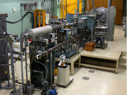
This facility permits material irradiation either by a 2 MeV electron beam or by Bremsstrahlung induced by stopping the electron beam. In this way, radiation testing that is normally carried out using a Co-60 source can be undertaken more rapidly (producing a larger and better controlled dose rate) while allowing in-situ measurements. Irradiation parameters (temperature, vacuum pressure, gas environment, dose rate and beam energy) are well controlled. Moreover, irradiation of relatively large components or material samples is possible. The accelerator staff can design and develop different irradiation chambers and experimental set-ups depending on irradiation requirements. Such experimental systems permit performing optical, electrical and dielectrical measurements during irradiation ("in-beam"). This makes it a unique experimental radiation facility in which simultaneous optical, electrical and dielectrical measurements can be made in the range of Hz to GHz. For this, systems to measure optical absorption and radioluminescence, electrical conductivity and dielectric properties during irradiation (in-situ) are mounted on the accelerator beam line.
Beam characteristics;
Electron energy: 0.25 to 2.0 MeV. Beam current: 10 pA to 150 µA
Sample size from ≈ 3 mm2 to about 20x20 cm2.
Unfocused beam diameter at target is ≈ 1 cm
Beam can be focused to ≈ 1 mm diameter (for small samples)
Beam can be defocused to ≈ 3 cm diameter
Beam can be scanned over 20x20 cm2 (for large samples)
The facility has been used for studying insulators for which low displacement per atom (dpa) rates are required. The facility allows in-beam testing at a controlled temperature of the electrical, dielectric (RF), and optical properties of solid and gas insulators. Irradiation can be performed in high vacuum, air, or controlled atmospheres (such as N or He).
For insulator studies typical dpa rates range from about 10-12 to 10-8 dpa/s while ionization rates (Bremsstrahlung or direct electron irradiation) range form 0 to ≈ 104 Gy/s For steels, about 10-3 dpa/day can be achieved in samples of approximately 3x3x1 mm3.
Flexibility
The facility is extremely flexible and has several unique in-beam systems for measuring electrical conductivity, dielectric loss and permittivity (Hz to GHz), and optical absorption and emission during irradiation over a wide range of dose rates and temperatures. Irradiations can be performed in high vacuum, air, or controlled atmosphere such as N or He. Simulation in electron accelerators offers important advantages, namely easy experimental parameter control and high dose rates available (0 a ≈105 Gy/s).
In-situ measurement capability and expertise. To date a range of studies have been carried out on fusion candidate insulators. For instance, electrical, optical as well as hydrogen and helium diffusion properties are measured during irradiation. These studies are carried out at a controlled temperature, from liquid nitrogen up to 1000 C. For these studies special irradiation chambers and sample holders have been designed by the accelerator staff and have been fabricated at the Ciemat workshops.
60 keV DANFYSIK ION IMPLANTER
This facility permits ion implantation at energies up to 60 keV. For instance, helium, hydrogen and duterium ions have been implanted for a range of studies related with fusion research. The implanter staff have designed and developed different irradiation chambers and experimental set-ups depending on the study requirements. The developed experimental systems permit in-situ optical, electrical and desorption measurements. For instance simultaneous ionoluminescence and surface electrical conductivity measurements can be made thus allowing correlation between macroscopic material degradation and defects produced by implantation.
Beam characteristics;
- Beam energy: up to 60 keV.
- Beam current: up to 150 µA depending on ion.
- Sample size: from ≈ 3 mm2 to about 4x2 cm2
- Unfocused beam diameter at target: ≈ 1 cm
The facility has been used regularly to implant H, He, D ions in metals and insulators in order to evaluate microstructural surface degradation, ionoluminescence, surface electrical degradation and to implant He and H isotopes to perform diffusion and desorption experiments. These studies can be carried out at controlled temperatures, from liquid nitrogen up to 1000 C. Available special irradiation chambers and sample holders have been designed by the implanter staff and fabricated at the Ciemat workshops.
NAYADE Co-60 irradiation facility
For gamma rays irradiations CIEMAT has the ownership of a Co-60 facility with unrestricted access. The irradiations can be performed for long periods. The Nayade facility of CIEMAT is pool-type with water as biological shield. It consists of a pool of 1.2 m on side and 4.5 m deep of water, providing enough biological shielding for about 100,000 Ci of Co-60. The pool has the equipment and systems necessary to ensure safety controls through water level, radiation detectors, control of water purity through pH and conductivity measurements. These devices are controlled in a common console. The use of water as a biological shield allows direct vision of the bottom pool that is the surface where the radiation produced and facilitates the moving and positioning the sources and extraction of samples in the different devices.
The main irradiation characteristics in Nayade are:
- Type of source; 60Co cylindrical sources (15 mm diam. x 135 mm long)12 sources are distributed in a circular way providing an inner cylindrical irradiation volume.
- Two distributions are available:1.High flux; ≤ 8.3 103Gy/h within a 60mm diameter x 100 mm long volume. 2.Low flux; ≤ 1.2x10² Gy/h within a 200 mm diameter x 100 mm long volume (in the low flux configuration the sources rotate on an outer circle for uniform dose.
- Irradiations at controlled temperatures and atmospheres, together with in-situ testing of electrical properties are also possible.
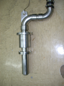
- In this device the irradiations can be carried out at controlled temperature up to 300ºC. A gas flow (as dry air or nitrogen) can be introduce during the irradiations to prevent possible effect of humidity. The uncertainty dose rate is better than 20% in a volume about 283 cm3. A picture of the irradiation chamber (out of the irradiation pool) can be seen in figure.
Irradiation rigs are rotinously fabricated at Ciemat workshops in order to perform irradiations at different dose rates and conditions and to perform measurements during irradiations. The equipment and devices required to perform the irradiation tests, as sensors, signal cables, standard laboratory equipment, feedthrough, environmental monitors (temperature, pressure, humidity, radiation) are available Hardware and software with the function to acquire, record, transfer, store and process data acquired with the equipment of the irradiation test are available.
- Dosimetry system
The routine gamma dosimetry is performed using the commercially available Red Perspex™ 4034 Harwell dosimeters, they are polymethylmethacrylate (PMMA) dosimeters that have become widely used in routine high-dose rate dosimetry in the field of the industrial radiation processing. When exposed to ionising doses in excess of 1 kGy, the Red 4034 polymer starts to darken due to the formation of a new absorption band peaking at 615 nm and extending from 600 nm to beyond 700 nm. The absorbed dose is therefore determined by measuring its radiation-induced absorbance in the 630nm-650 nm range where post-irradiation fading is minimal. 640 nm wavelength is used as read-out wavelength. The absorbance per unit thickness, expressed in cm−1, is the dose-dependent quantity measured against air as reference. These dosimeters has been shown to be valid in the range of 5 to 50 kGy and its accuracy is better than 10 per cent. The Red 4034 dosimeters are pre-conditioned in a fixed humidity environment and hermetically sealed in polyester/aluminium foil/polyethylene laminate pouches, as absorbed water concentration was identified as a parameter which could influence the spectrophotometric response and hence the dose readout. Keeping the dosimeter in its packaging is mandatory to use the calibration curves (absorbance at 640nm (cm-1) related to dose) supplied by the manufacturer. The temperature sensitivity of the dosimeter is the most important environmental dependance. From a practical point of view, the Red 4034 dosimeters are temperature-independent up to 40 ºC, provided that the measurements are made shortly after the end of the irradiation These dosimeters have been also used to measure gamma dose in BR1 graphite-moderated,air-cooled nuclear reactor (SCK·CEN MOL), in mixed gamma neutron fields at a temperature below 40º. A gamma dosimetry before to start the irradiation test is always carried out.
Material Characterization Facilities
Focused Ion Beam - Secondary Electron Microscope (FIB-SEM)
This is Carl Zeiss Auriga Compact field effect SEM with an electron acceleration voltage in the range 0.5 to 30 kV and is equipped with three different detectors for secondary and backscattered electrons. The system includes an XFlash Bruker EDS detector for compositional studies. It is possible to perform local point, line scan and mapping analysis. An electron back-scattered diffraction detector (EBSD) has been recently installed for the determination of crystalline phases and orientation with a sample angle of 70º. The microscope is also equipped with an FIB gallium gun providing an acceleration voltage of 1 to 30 keV for cross-section inspection and TEM samples preparation on conductive and insulating materials.
Secondary Ion Mass Spectrometry (SIMS)
SIMS: Hiden Analytical secondary ion mass spectroscopy equipment using oxygen or argon ions as primary ions with an energy of 5 keV. Mass identification (1 to 550 amu), depth profiling and static SIMS capabilities. The system is also useful for compositional mapping and it incorporates an electron gun for SIMS experiments in insulating materials. The electronegative ions can be better detected using a Cs ion gun, with an energy up to 5 keV.
